The world runs on information, with humanity creating an estimated 2.5 million terabytes of data per day. However, all this data is useless unless we can process it, so, arguably, one of the things that the modern world cannot live without is processors.
But how is a processor made? Why is it a modern marvel? How can a manufacturer fit billions of transistors into such a small package? Let's dive deep into how Intel, one of the largest chip manufacturers globally, creates a CPU from sand.
Extracting Silicon From Sand

The base ingredient of any processor, silicon, is extracted from desert sand. This material is found abundantly in the earth's crust and consists of around 25% to 50% silicon dioxide. It is processed to separate silicon from all other materials in the sand.
The processing repeats several times until the manufacturer creates a 99.9999% pure sample. The purified silicon is then poured to form a cylindrical electronic-grade ingot. The cylinder's diameter is 300mm and weighs about 100kg.
The manufacturer then slices the ingot into 925-micrometer-thin wafers. Afterward, it's polished to a mirror-smooth finish, removing all flaws and blemishes on its surface. These finished wafers are then shipped to Intel's semiconductor fabrication plant for transformation from a slab of silicon into a high-tech computer brain.
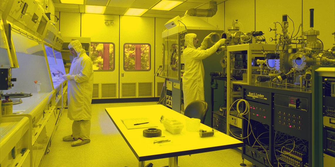
The FOUP Highway
As processors are high-precision parts, their pure silicon base mustn't be contaminated before, during, or after manufacturing. This is where the front-opening unified pods (FOUPs) come in. These automated pods hold 25 wafers at a time, keeping them safe and secure in an environmentally-controlled space when transporting the wafers between machines.
Furthermore, each wafer can travel through the same steps hundreds of times, sometimes going from one end of the building to the other. The entire process is embedded within the machines so that the FOUP knows where to go for each step.
Also, the FOUPs travel on monorails hanging from the ceiling, allowing them to take the fastest, most efficient part from one manufacturing step to another.
Photolithography

The photolithography process uses a photoresist to imprint patterns on the silicon wafer. Photoresist is a tough, light-sensitive material similar to what you find on film. Once this is applied, the wafer is exposed to ultraviolet light with a mask of the processor's pattern.
The mask ensures that only the places they want to process are exposed, thus leaving the photoresist in that area soluble. Once the pattern is fully imprinted on the silicon wafer, it goes through a chemical bath to remove all the exposed photoresist, leaving a pattern of bare silicon that will go through the next steps in the process.
Ion Implantation
Also known as doping, this process embeds atoms from different elements to improve conductivity. Once complete, the initial photoresist layer is removed, and a new one is put in place to prepare the wafer for the next step.
Etching
After another round of photolithography, the silicon wafer heads on to etching, where the processor's transistors start to form. Photoresist is applied to areas where they want the silicon to remain, while the parts that must be removed are chemically etched.
The remaining material slowly becomes the transistors' channels, where the electrons flow from one point to another.
Material Deposition
Once the channels have been created, the silicon wafer returns to photolithography to add or remove photoresist layers as needed. It then proceeds to material deposition. Various layers of different materials, like silicon dioxide, polycrystalline silicon, high-k dielectric, different metal alloys, and copper, are added and etched to create, finalize, and connect the millions of transistors on the chip.
Chemical Mechanical Planarization
Every processor layer undergoes chemical mechanical planarization, also known as polishing, to trim off excess materials. Once the topmost layer is removed, the underlying copper pattern is revealed, allowing the manufacturer to create more copper layers to connect the different transistors as required.
Although processors look impossibly thin, they usually have more than 30 layers of complex circuitry. This allows it to deliver the processing power required by today's applications.
Testing, Slicing, and Sorting
A silicon wafer can go through all the above processes to create a processor. Once the silicon wafer completes that journey, it then begins testing. This process checks each created piece on the wafer for functionality—whether it works or not.
Once done, the wafer is then cut into pieces called a die. It's then sorted, where dies that work move forward to packaging, and those that fail are discarded.
Turning the Silicon Die Into a Processor

This process, called packaging, transforms dies into processors. A substrate, typically a printed circuit board, and a heat spreader are put on the die to form the CPU you buy. The substrate is where the die physically connects to the motherboard while the heat spreader interfaces with your CPU's DC or PWM cooling fan.
Testing and Quality Control

The completed processors are then tested again, but this time for performance, power, and functionality. This test determines what kind of chip it will be—whether it's good to be an i3, i5, i7, or i9 processor. The processors are then grouped accordingly for retail packaging or placed in trays for delivery to computer manufacturers.
Microscopically Small Yet Immensely Complicated
While processors look simple from the outside, they're immensely complicated. Processor manufacturing takes two and a half to three months of 24/7 processes. And despite the highly-precise engineering behind these chips, there's still no guarantee they'll get a perfect wafer.
In fact, processor makers can lose somewhere between 20% and 70% of the dies on a wafer due to imperfections, contaminants, and more. This value is further impacted by increasingly small CPU processes, with the newest chips going as small as 4nm.
However, as Moore's Law states, we can still expect processor performance to double every two years until 2025. Until processors hit the fundamental ceiling of atom size, all these manufacturing processes must cope with the designs to produce the chip we demand.