Moore's Law is one of those miracles of modern life that we all take for granted, like grocery stores and dentistry with anesthesia.
For 50 years now, computer processors have been doubling their performance per dollar per square centimeter every 1-2 years. This exponential trend has taken us from the ENIAC's 500 flops (floating point operations per second) to around 54 petaflops for the most powerful supercomputer today, the Tianhe-2. That's about a ten trillion fold improvement, in well under a century. That's incredible by anyone's reckoning.
This achievement has been happening so reliably, for so long, that it's become a mundane truth about computing.
We take it for granted.
Which is why it's so scary that it could all come to a stop in the near future. A number of fundamental physical limits are converging to put a stop to the progression of traditional silicon computer chips. While there is theoretical computing technology that could solve some of these problems, the fact remains that progress is currently slowing down. The days of exponentially improving computers could be coming to a close.
But not quite yet.
A new breakthrough from IBM shows that Moore's law still has legs. A research group lead by the company has shown off a prototype for a processor with transistor components just 7 nanometers wide. This is half the size (and quadruple the performance) of current 14 nanometer technology, pushing the demise of Moore's Law out to at least 2018.
So how was this breakthrough achieved? And, when can you expect to see this technology in real devices?
Old Atoms, New Tricks
The new prototype isn't a production chip, but it has been produced with commercially scalable techniques that could go to market in the next few years (rumor has it that IBM would like the chip to premier in 2017-2018. The prototype is the product of IBM/SUNY, an IMB research lab that cooperated with the State University of New York. A number of companies and research groups collaborated on the project, including SAMSUNG and Global Foundries, a company which IBM is paying roughly 1.3 billion dollars to take over its unprofitable chip fabrication wing.
Basically, IBM's research group made two key improvements that made this possible: developing a better material, and developing a better etching process. Each of these overcome a major barrier to the development of denser processors. Let's look at each of these in turn.
Better Material
One of the barriers to smaller transistors is simply the shrinking number of atoms. a 7nm transistor has components that are only about 35 silicon atoms across. In order for current to flow, electrons need to physically jump from one atom's orbital to another's. In a pure silicon wafer, as has traditionally been used, it's hard or impossible to get sufficient current to flow through such a small number of atoms.

To solve this problem IBM had to abandon pure silicon in favor of using an alloy of silicon and germanium. This has a key advantage: it increases so-called "electron motility" -- the ability of electrons to flow through the material. Silicon begins to function poorly at the 10 nanometer scale, which is one of the reasons that efforts to develop 10 nm processors have stalled. The addition of germanium leapfrogs this barrier.
Finer Etching
There's also the question of how you actually shape objects that tiny. The way computer processors are produced is using extremely powerful lasers, and various optics and stencils to carve out tiny features. The limitation here is the wavelength of the light , which imposes a limit on how finely we can etch features.
For a long time, chip fabrication has stabilized around using an argon fluoride laser, with a wave-length of 193 nanometers. You may notice that this is quite a bit larger than the 14 nanometer features we've been etching with. Fortunately, the wave length is not a hard limit on resolution. It is possible to use interference and other tricks to eke out more precision. However, chipmakers have been running out of clever ideas and now a major change is needed.

IBM's take on that idea has been to use an EUV light source (Extreme Ultra Violet), with a wavelength of just 13.5 nanometers. This, using similar tricks to those we used with argon-fluoride, should give us an etching resolution of just a couple of nanometers with more development.
Unfortunately, it also requires throwing out most of what we know about chip fabrication, as well as most of the technological infrastructure developed for it, one of the reasons that the technology took so long to come into its own.
This technology opens the door to continuing the development of Moore's Law all the way down to the quantum limit -- the point at which the quantum uncertainty around the position of an electron is larger than the transistor itself, causing processor elements to behave randomly. From there, truly new technology will be required to push computing further.
The Next Five Years of Chip Fabrication

Intel is still struggling to produce a viable 10nm processor. It's not out of the question that IBM's coalition could beat them to the punch. If that happens, it'll indicate that the balance of power in the semiconductor industry has finally shifted away from Intel.
The future of Moore's Law is uncertain. However the story ends, it will be tumultuous. Kingdoms will be won and lost. It'll be interesting to see who winds up on top when all the dust settles. And, in the short term, it's nice to know the unstoppable march of human progress won't be petering out for at least another few years.
Are you excited for faster chips? Worried about the end of Moore's Law? Let us know in the comments!
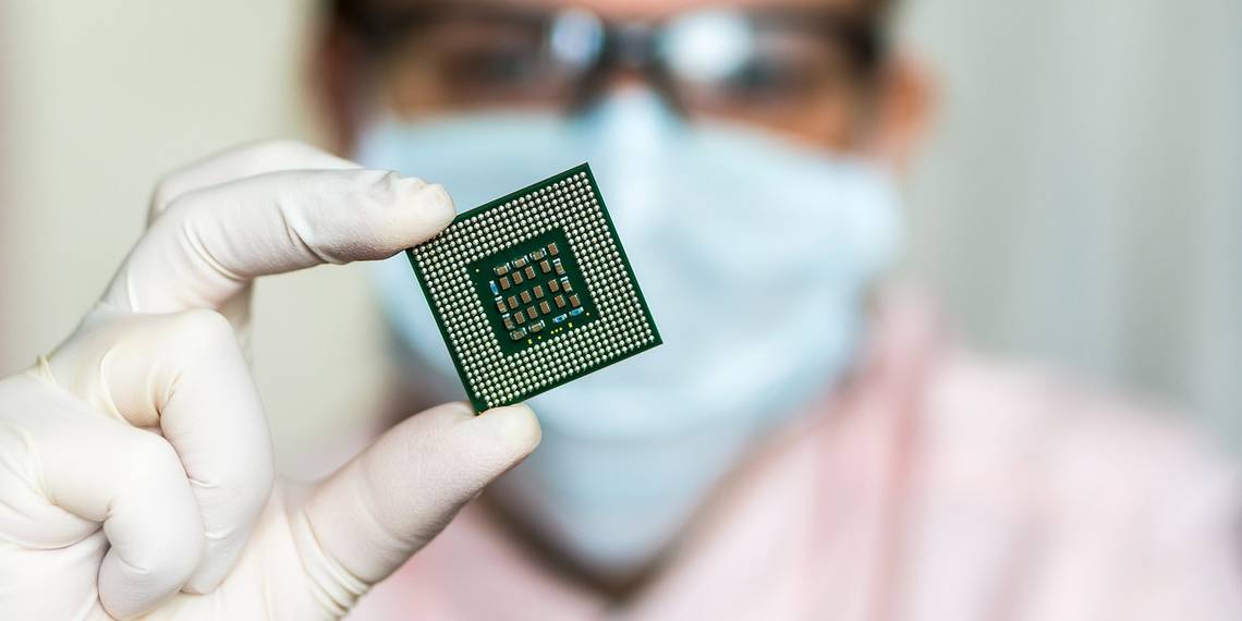
Image Credits: computer microchip via Shutterstock, "Silicon Croda", "Argon-Ion Laser," "Logotype Intel," by Wikimedia